Page 24 - CFM_Newsletter_CY22
P. 24
Epitaxial III-nitrides nanostructures for optoelectronic applications

        Dr. Sunil S. Kushvaha, CSIR-National Physical Laboratory, New Delhi, November 30                         th

        Dr.  Sunil  Singh  Kushvaha,  Principal  Scientist,  CSIR-National  Physical
        Laboratory, Delhi discussed epitaxial III-nitrides nanostructures for optoelectronic
        applications.  Among  various  semiconducting  materials,  III-nitrides  (AlN,  GaN,
        InN,  and  their  alloys)  semiconductors  stand  out  as  one  of  the  most  popular
        materials  due  to  their  excellent  physical  and  physical  and  optoelectronic
        properties. The speaker discussed about the various GaN nanostructures such
        as nanorods, porous NWN, islands and thin films that were grown using laser
        assisted  molecular  bean  epitaxy  (LMBE)  on  sapphire-based  substrates  and
        flexible metal foils. Their team fabricated metal-semiconductor-metal (M-S-M) UV
        photodetectors on GaN thin film, nano-columns and nanowall networks grown on
        GaN sapphire-based substrates. They also conducted the PEC measurement on
        GaN NCs on Nb foils under standard conditions showed the effective photo-catalyst nature and observed
        an enhancement in PEC efficiency in the case of reduced graphene oxide film coated on GaN NCs. The
        speaker concluded the talk by explaining the properties exhibited by hybrid GaN nanostructures which are
        suitable for fabricating efficient optoelectronic devices.


        Importance of Understanding Ultrafast Reactions in Energy Conversion


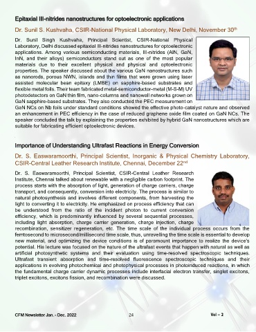
        Dr.  S.  Easwaramoorthi,  Principal  Scientist,  Inorganic  &  Physical  Chemistry  Laboratory,
        CSIR-Central Leather Research Institute, Chennai, December 22
                                                                                         nd
        Dr.  S.  Easwaramoorthi,  Principal  Scientist,  CSIR-Central  Leather  Research
        Institute, Chennai talked about renewable with a negligible carbon footprint. The
        process starts with the absorption of light, generation of charge carriers, charge
        transport, and consequently, conversion into electricity. The process is similar to
        natural photosynthesis and involves different components, from harvesting the
        light to converting it to electricity. He emphasized on process efficiency that can
        be  understood  from  the  ratio  of  the  incident  photon  to  current  conversion
        efficiency,  which  is  predominantly  influenced  by  several  sequential  processes,
        including  light  absorption,  charge  carrier  generation,  charge  injection,  charge
        recombination,  sensitizer  regeneration,  etc.  The  time  scale  of  the  individual  process  occurs  from  the
        femtosecond to microsecond/millisecond time scale, thus, unravelling the time scale is essential to develop
        new  material,  and  optimizing  the  device  conditions  is  of  paramount  importance  to  realize  the  device's
        potential. His lecture was focused on the nature of the ultrafast events that happen with natural as well as
        artificial  photosynthetic  systems  and  their  evaluation  using  time-resolved  spectroscopic  techniques.
        Ultrafast  transient  absorption  and  time-resolved  fluorescence  spectroscopic  techniques  and  their
        applications in evolving photochemical and photophysical processes in photoinduced reactions, in which
        the fundamental charge carrier dynamic processes include interfacial electron transfer, singlet excitons,
        triplet excitons, excitons fission, and recombination were discussed.


        CFM Newsletter Jan. – Dec. 2022                         24                                    Vol – 2

