PI Name & Affiliation:
Dr. Ashutosh Mahajan
Associate Professor
Centre for Nanotechnology Research,
School of Electronics Engineering
Co-PI Name & Affiliation:
Dr. Rajan Kumar Pandey
Associate Professor
SSchool of Electronics Engineering
Funding Agency: Science and Engineering Research Board (SERB),
Scheme: Core Research Grant (CRG)
Overlay: Rs. 49,83,471
Duration of the Project: 3 Years

Dr. Ashutosh Mahajan

Dr. Rajan Kumar Pandey
Graphical Abstract

Project Description
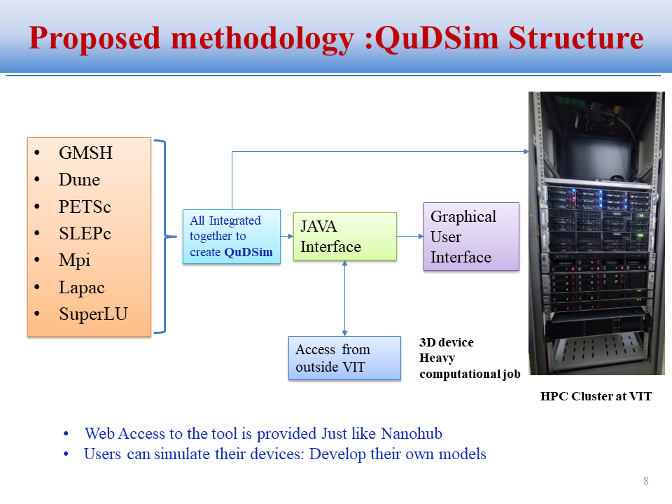
The main advantage of the development FEM device simulator is the Flexibility it can offer. The Device simulation user and developers can modify and create physical parameters, boundary conditions, or incorporate a set of additional governing equations. Parameters like effective mass and Bandgap enhancement can be calculated using DFT computation (atomistic modelling) and made available to the device simulator. Commercial tools have these parameters that are free and not always fixed by physical principles. Another advantage is that users can make maximum use of the computational resource available by tuning the complexity of the problem to be solved either by changing the refinement of the grid, incorporating additional differential equations. Simulation tool suitable to study devices other than NS-FET such as emerging non-volatile Flash memory devices and for other materials such as III-V semiconductors. An open-source device simulation tool can be accessed from users outside VIT.
Products/ Instruments/ Results/ Outreach Activities (Pictures)
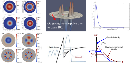
Self-consisten simulation of cylindrical GAA structure/ Methodology/ Wavefunctions of electrons/ Charge Density
